By Dr. Ann Kelleher, Executive Vice President and General Manager of Technology Development, Intel
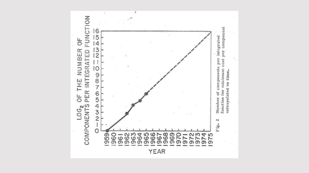
Figure 1: Original graph from “Cramming more components onto integrated circuits” 1
In 1965, Intel co-founder Gordon Moore predicted that the number of transistors on a chip would double roughly every two years, with a minimal rise in cost. This prediction became known as Moore’s Law and is depicted in Figure 1. The more transistors or components on a device, the cost per device is reduced while the performance per device is increased.
The rate of digitalization of the world surged over the past two years, triggered by the COVID-19 pandemic, and this enhanced transition was enabled by the semiconductor industry and its innovation.
Intel CEO Pat Gelsinger has shared: “Technology has never been more important for humanity than it is now. Everything is becoming digital, with four key superpowers.” The superpowers – ubiquitous computing, cloud-to-edge infrastructure, pervasive connectivity and artificial intelligence – are set to transcend and transform the world. At this time we see no end to the demand for compute, and more compute continues to push the industry for more innovation. For example, the world creates nearly 270,000 petabytes (i.e. 27 x1019) of data every day. We are projecting that by the end of this decade, on average, all of us will have 1 petaflop (1015 floating-point operations per second) of compute and 1 petabyte of data less than 1 millisecond away. This demand for more and more computing power is the push for the industry to maintain the pace of Moore’s Law.
For over 40 years, Intel engineers have continually innovated to squeeze more and more transistors onto ever-smaller chips and maintain the pace of Moore’s Law. In the mid to late 2010s, as it has several times before, the industry predicted that “Moore’s Law is dead.” To paraphrase a famous saying, I feel the reports of the death of Moore’s Law are greatly exaggerated. Innovation is not dead, and we will maintain Moore’s Law as we always have, through innovation – innovation in process, in packaging and in architecture. It will be a challenge as always – and Intel is up to the challenge.
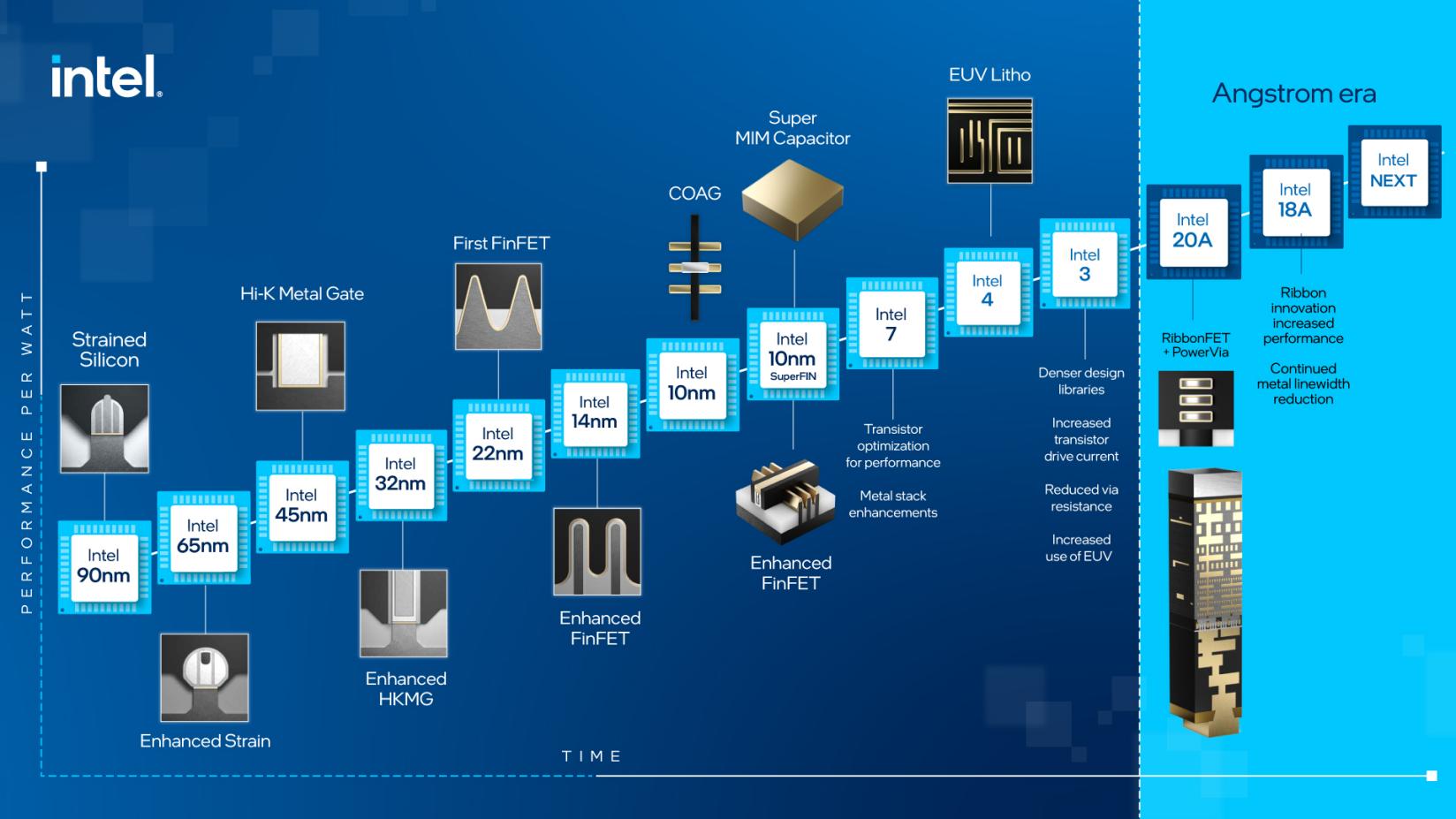
Figure 2: Transistor innovations over time
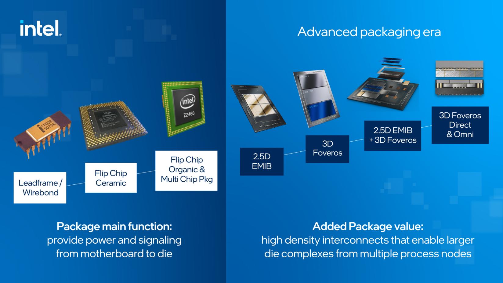
Innovation Today: Process
Intel has a long, rich history of foundational process innovations in pursuit of Moore’s Law, as seen in Figure 2. Intel engineers and scientists have continually faced — then overcome — the challenges posed by physics when the features on a chip shrink to the size of atoms. With inventions such as high-k metal gate technology, tri-gate 3D transistors and strained silicon, Intel has consistently delivered groundbreaking technologies to maintain pace with Moore’s Law. By the late 2000s, as physical dimensions continued to shrink, the industry realized that additional areas of innovation, including materials science, new process architecture and design technology co-optimization (DTCO), were needed to keep pace.
Intel’s next great architectural innovation is RibbonFET, our implementation of the gate-all-around (GAA) transistor, arriving with Intel 20A. RibbonFET represents our first new transistor architecture since FinFET. RibbonFET delivers faster transistor switching speeds with the same drive current in a smaller footprint. At the same time, we also deliver PowerVia, the industry’s first backside power delivery architecture. Previously, power came from the top of the die and “competed” with signal interconnects. By separating power and signal, you can use the metal layers more effectively, as there are fewer trade-offs to make. This results in improved performance. The next generation of extreme ultraviolet (EUV) lithography, High Numerical Aperture or “High NA,” brings further improvements in resolution and error reduction, delivering a reduction in process complexity with an increased flexibility in design rules. Intel is in close partnership with ASML and other ecosystem partners to be the first to bring this technology into high-volume production.
These examples are just the beginning. After the introduction of RibbonFET and PowerVia with Intel 20A and Intel 18A, new follow-on process nodes are already in development delivering additional gains in power, performance and density. These gains are achieved through several innovations, including backend metal resistance and capacitance improvements, transistor architecture and library architecture improvements. As we said in July 2021, as we implement these innovations and others, we expect to achieve transistor performance per watt parity by 2024 and leadership by 2025.